
The University of Iowa's DEC PDP-8Restoration Log
Part of
the UI-8 pages
|
The University of Iowa's DEC PDP-8Restoration Log
Part of
the UI-8 pages
|
This is a chronological log of the progress restoring the University of Iowa's PDP-8 computer. Entries are added at the end as work progresses. Click on any thumbnail image to see full-sized image.
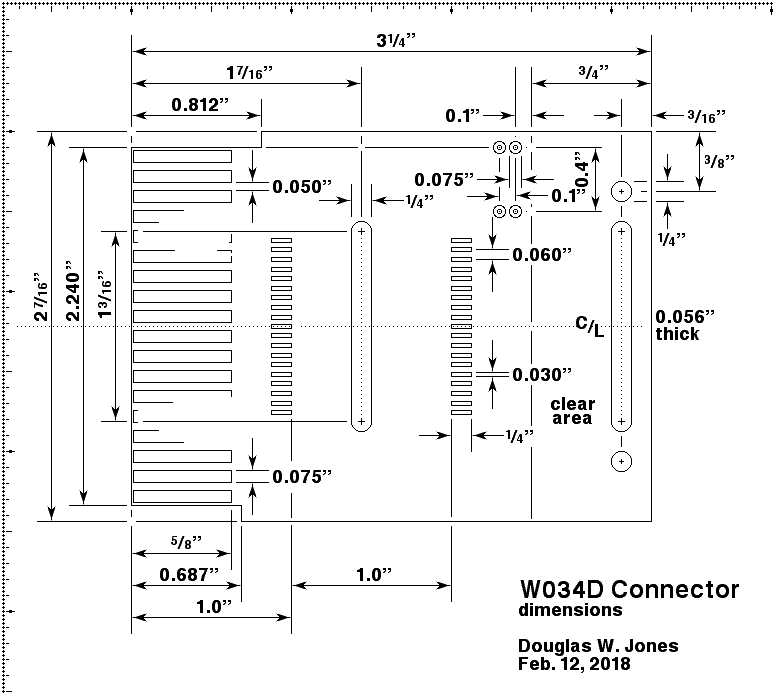
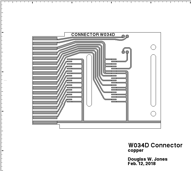
Bug 4 and Bug 64: Given that quite a bit of the the CPU seems to be working, we began to investigate the memory. One of the first things we noticed was that the Maintenance Manual (Feb. 1966 Ed., pages 10-70 to 10-76) documents 7 W034 cables between the CPU and memory half backplanes, but there are only 6 present. The missing cable (page 10-76) would connect backplane slots PD02 and MD35. While we have not fully understood the signals that pass through the various cables, this makes it more pressing that we attempt to manufacture replacements for these cables.
|
|
| W034D cable connector | |
|---|---|
Having done this, we found that Vince Slyngstad has already done much of this.
See his
CAD Project Files,
indexed under ./DEC/Wxxx/W034: Flexprint, 16 connections on "B" side 10
ohms on A2, B2. This includes photos, schematics and board layouts for
the W034D, W034H, and W034X. The latter is a modern redesign, while the two
former are historical DEC designs. We need to evaluate his modern design to
see if it meets our requirements.
Bug 31: After poking around the ADC rack, we decided to remove the locally built magnetic tape drive interface from the ADC rack. Removal of this device interface is complicated by the fact that it is not daisy-chained into the I/O bus the way off-the-shelf device interfaces were done. Instead, wire-wrap wiring has been used to tap into the I/O bus connectors in the analog to digital converter backplane immediately above it. In addition, spare slots in that backplane have been used for a few additional logic boards and interface plugs needed for the tape drive.
|
| Using an unwrapping tool |
|---|
Pin E12B refers to a pin on row E (counting from the top), slot 12 (counting from the left side of the wiring side of the backplane) pin E (as printed in white on the wiring side of the black connector blocks). The tape-drive interface was mostly in rows E and F, with wiring to a few spare slots in row D and one slot (used for a cable connector) in row C. We logged the wire color, source pin and destination pin for each wire we removed.
We also pulled the cables that connected the tape-drive control panel to
slots in the backplane segments involved. The wires at one end of this
cable were soldered to parts of the control panel, another end of this
cable ended in cut-off wires that apparently went to the tape drive, while
the third and forth ends of this cable went to card-edge connectors plugged
into the backplane. At least one of these was almost certainly plugged into
the wrong backplane slot, but we wrote on each card-edge connector the slot
number into which it had been plugged.
|
| Removing rows E and F |
|---|
With the final wire removed, we were able to pull the remains of the home-brew tape-drive interface from the rack. We believe that some boards on the lower right end of row D are also part of this home-brew interface. Wiring to those boards from rows E and F has been removed, but the local wiring on row D remains in place.
The home-made tape drive control panel directly below rows E and F had one remaining cable still connecting it to other parts of the rack. In this case, to a block of relays attached to a board cantelevered out from the back of the topmost panel on the back of the rack. We simply cut the wires from the cable to this block of relays. The colors of the cut wires should be sufficient to allow reversing this change, should someone want to do so. We will tag all removed parts to allow this.
Bug 64: We tracked down David Gesswein's photos of a table-top PDP-8 he restored. These photos of his show the cabling between the two half backplanes:
These photos clearly show only 6 cables, all from Px01 to Mx36
(for x from A to F). The photos do not show the 7th cable connecting
PD02 to MD35.
On Feb. 12, 2018
we had speculated that perhaps this missing cable was the cause of our memory
problems. Apparently, this is not the case. It appears that this cable is
not needed on machines with only 4K of memory. Therefore, cable replacement
moves down on our list of prioritie, but remains there because of the decayed
nature of the 6 cables we have.
|
| Current limiters |
|---|
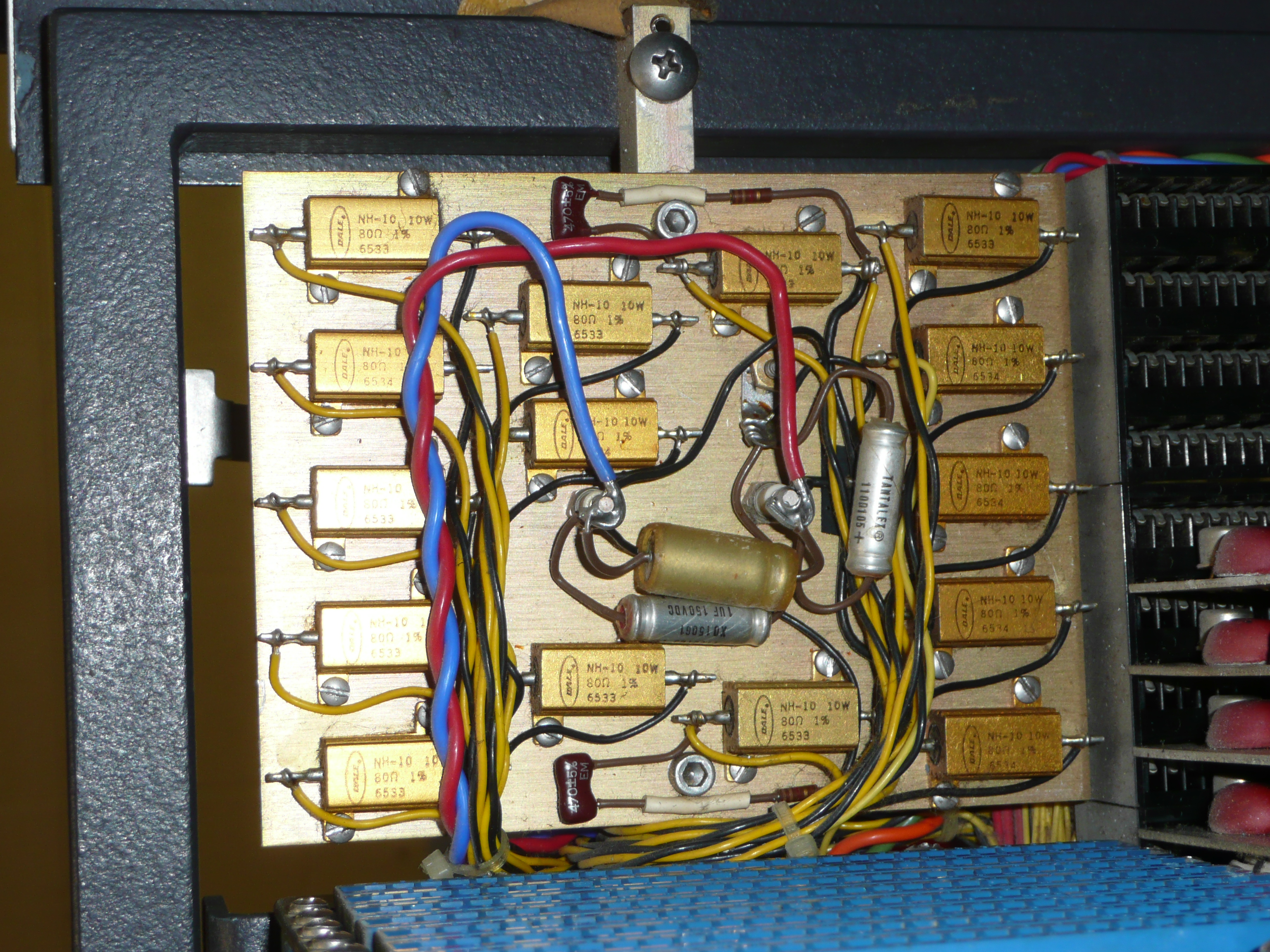
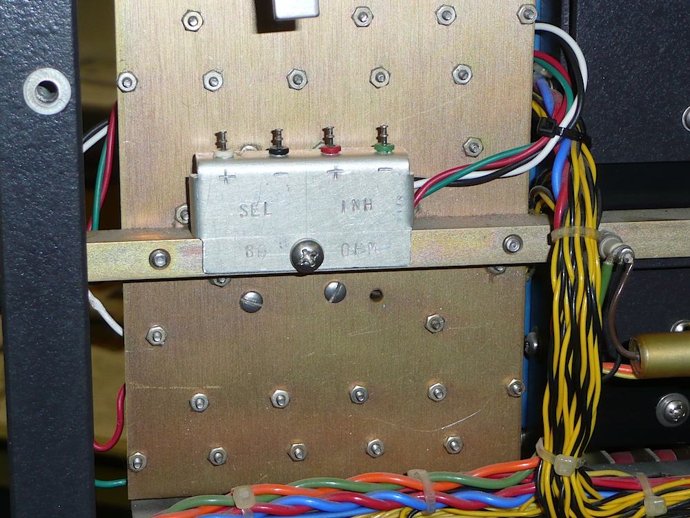
Looking at the detailed drawings in the Maintenance Manual, BS-D-8M-0-12 X Axis Selection, BS-D-8M-0-13 Y Axis Selection and BS-D-AM-0-15 Sense Amps, Inhibit Drivers, and Memory Control all show the detailed locations of the boards involved and document the role of 80&Ohm; current limiting resistors, but they don't show where the resistors are. We found these resistors lurking on an aluminum heat sink behind the balun network boards on the front-side of the core stack. See photo. These are all 80&Ohm; 10W 1% precision resistors. We infer from the fact that two of them have small resistor capacitor networks serving as shunts that those two are the X and Y axis current limiters attached to the G209 modules, while the other 13 resistors each serve one of the G208 inhibit drivers (the 13th resistor is a spare on our system since we don't have the memory parity option.) Note that this little RC network isn't documented in the maintenance manual.
A second problem we will face is that the above-cited manual pages all refer
to handwritten notes that should be on the label of our memory module. We have
found no such notes. The
Dalby Datormuseum
has a photo of the label on
their PDP-8
memory that gives a R/W (select) current of 325mA and an inhibit current of
305mA, so if we cannot find documentation for our machine, we at least know
reasonable values for these currents.
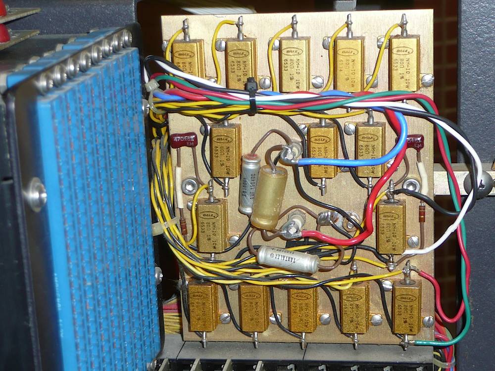
|
|
| Instrumented current limiters | |
|---|---|
An alternative way to measure the current through any of the 80Ω
resistors is to simply measure the voltage across the resistor, but they are
inaccessible behind the circuit boards holding the memory
balun coils.
To allow this method of measuring the current, we attached a set of 4 test
points at an accessible location directly behind the plate on which the
resistors are mounted and wired a pair of test points across one of the
resistors limiting the select current and one limiting the inhibit current.
|
|
| Inhibit and R/W select currents | |
|---|---|
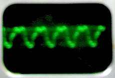
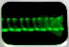
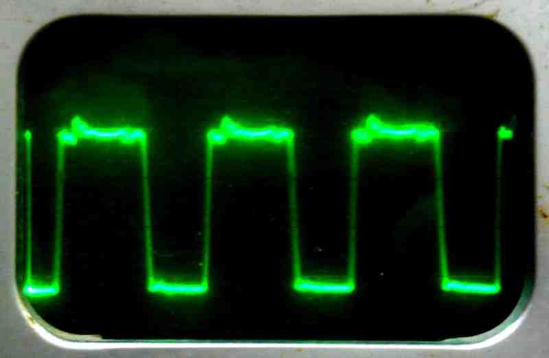
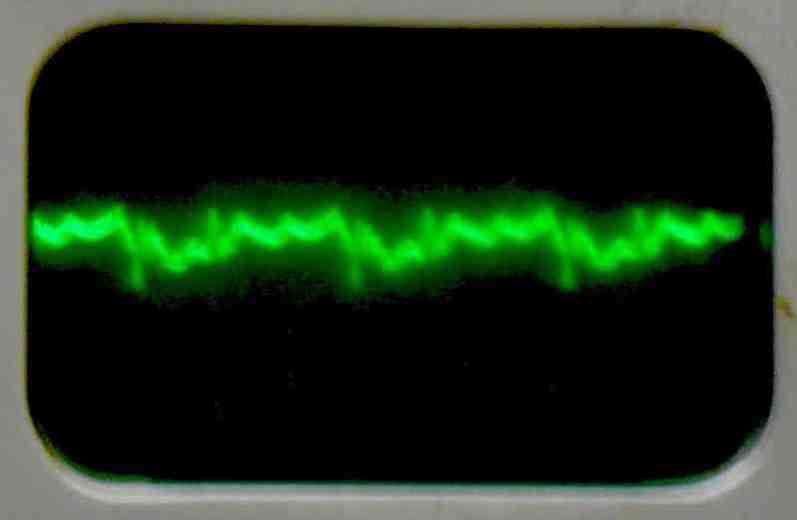
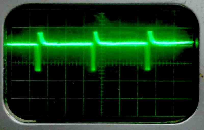
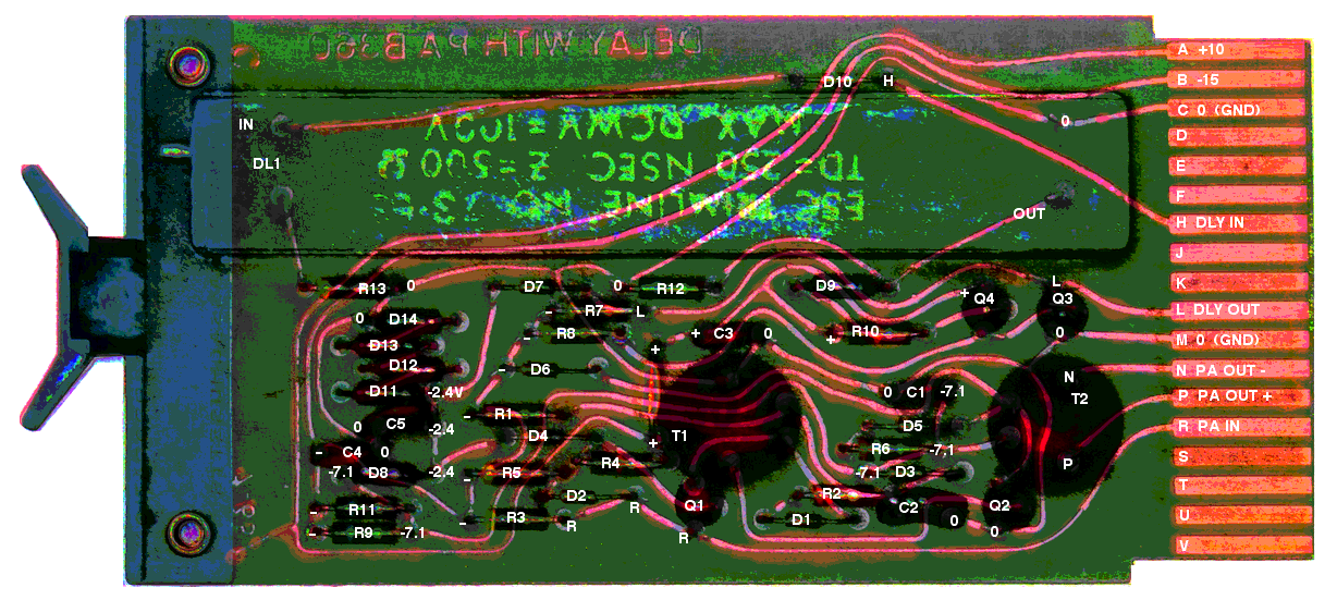
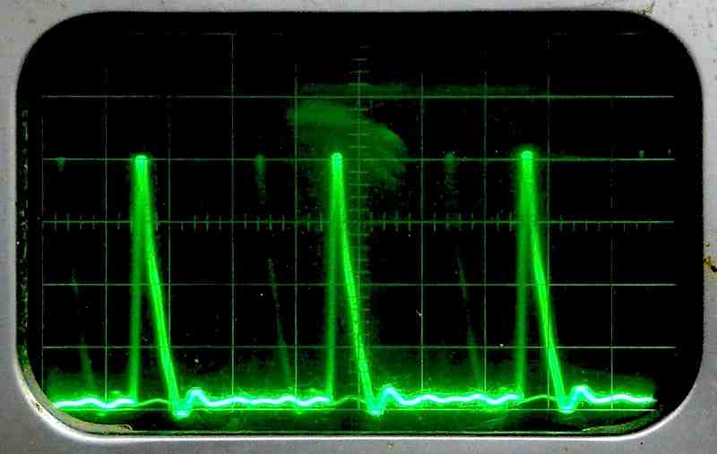
The good news is that we got waveforms on both the R/W select and inhibit currents. The waveforms start when you hit the CONT (continue) switch on the front panel, and they stop when you hit HALT. This means that the key memory control signals from the CPU are reaching the memory. This is the first time we have confirmed this.
Checking the scope by using its internal calibration oscillator, we found
that it was way out of calibration, so we spent the rest of the afternoon
searching the scope manual for calibration instructions and then doing
what we could to calibrate it using its internal calibration oscillator and
a DC voltmeter. The scope was, in fact, way out of calibration. The internal
10V DC supply from which the scope derives all of its other voltages was under
8 volts. Adjusting this and then bringing everything else into balance
seems to have made the scope trigger circuitry work much better.
|
|
| Inhibit and R/W select currents
1µsec/div hoiz; 10v/div vertical | |
|---|---|
The Dalby Datormuseum photo of their their PDP-8 memory label that gives a R/W select current of 325mA and an inhibit current of 305mA, so the values we see are in the right ballpark.
Because this is core memory, each memory cycle consists of a read/erase subcycle where the contents of the addressed word are destructively read, followed by a write/restore subcycle where the data just read is returned. The inhibit line is only pulsed during a write/restore cycle, and then, only when the value written is zero. Since we are currently reading all zeros from memory on every cycle, the inhibit line is pulsed once per cycle. This looks right.
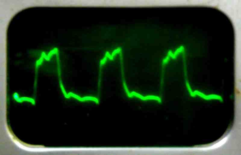
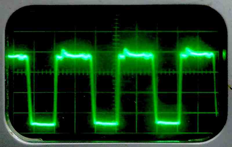
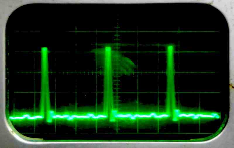
The R/W select lines are more complex. During the read/erase subcycle, the read select line should be pulsed, and during the write/restore subcycle, the write select line should be pulsed. These pulses are mixed by the balun networks on the G603 boards attached directly to the core memory module to produce a negative current pulse for the read/erase subcycle and a positive pulse for the write/restore subcycle. Both the read and write select lines in each pair share a single current limiting resistor, as shown in the Maintenance Manual (1965 ed, Figure 4-4, page 4-6). Thus, we should see two current pulses during each memory cycle, one for the read/erase subcycle, and one for the write/restore subcycle. We do see two pulses per subcycle, but they are strangely brief and they have different magnitudes! Something seems amiss.
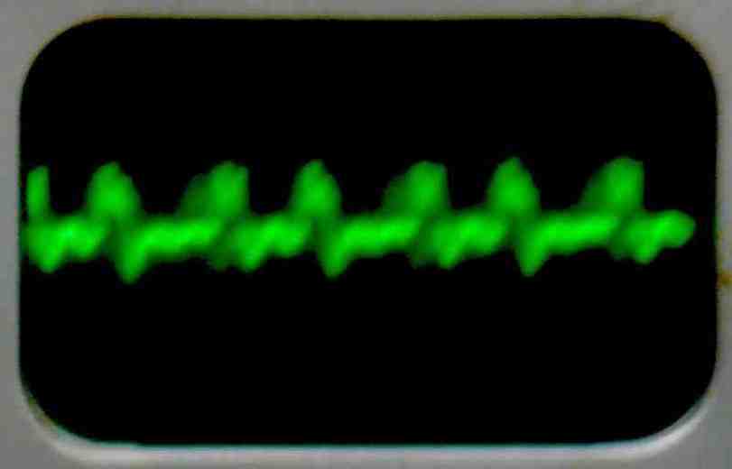
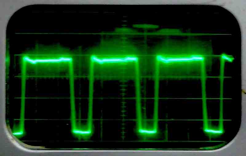
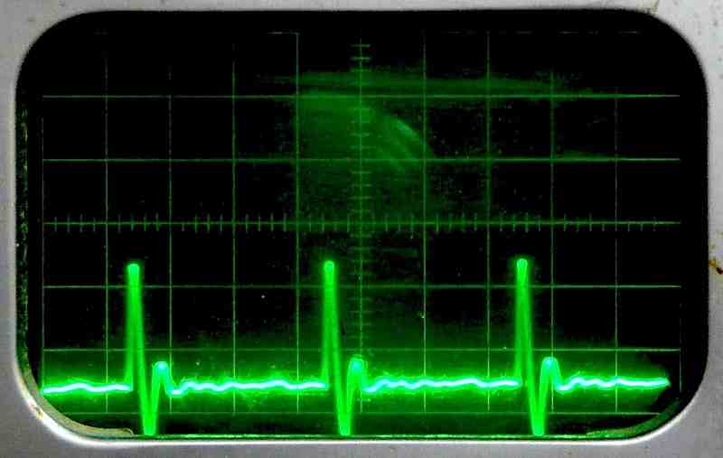
| |
| Inhibit logic signal | |
|---|---|
|
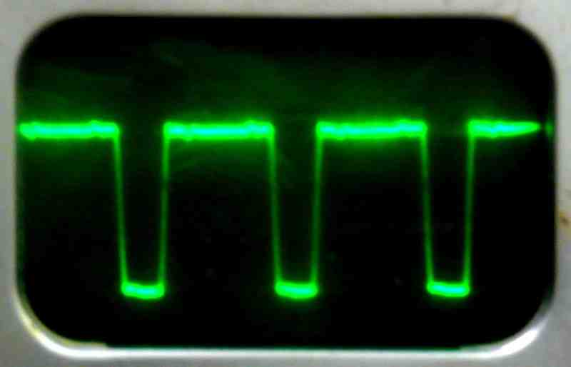
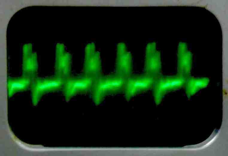
|
| Read and Write logic signals
1µsec/div hoiz; 1.0v/div vertical | |
We used internal triggering for these measurements, so do not read any
meaning into the phase differences on the scope displays.
|
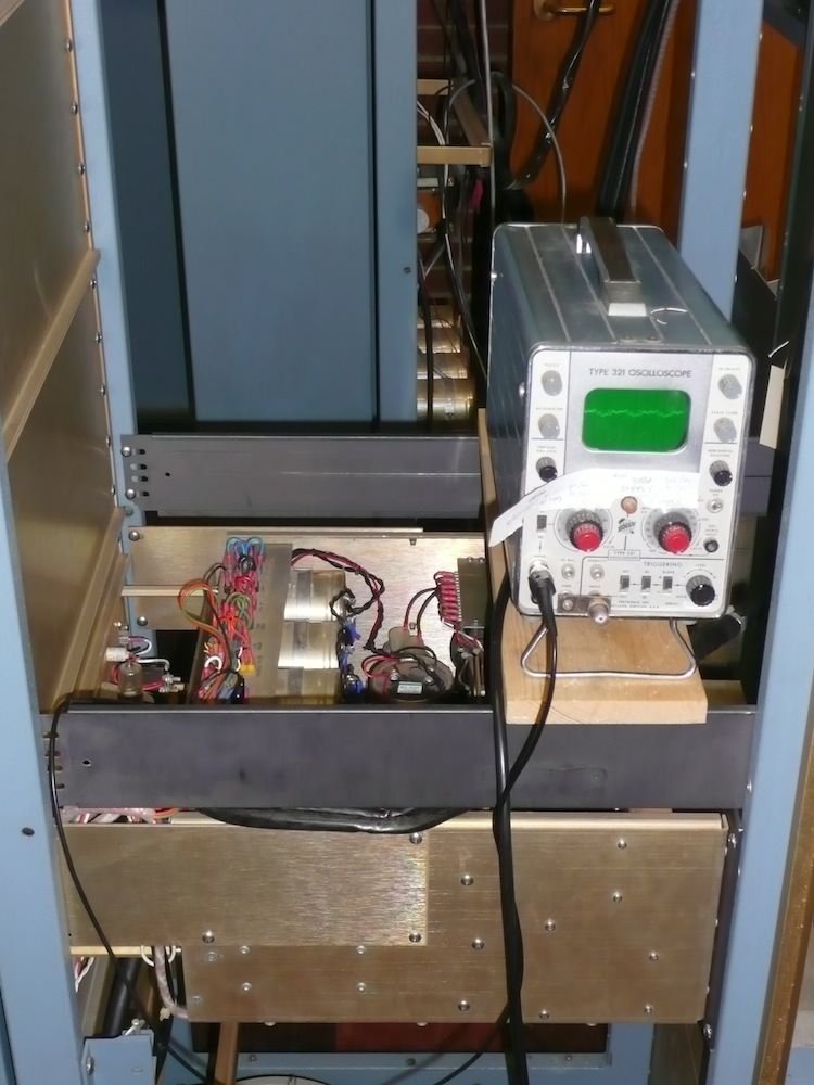
| Measuring supply ripple |
|---|
The photo shows our
oscilloscope
as used in these measurements. As mentioned on
Dec. 16, 2014,
the scope is set up for differential measurement, sitting on a dry wooden plank
to isolate it from ground and running from an isolated DC supply. This is
required because the inhibit and R/W select power supplies are not regulated
relative to ground.
|
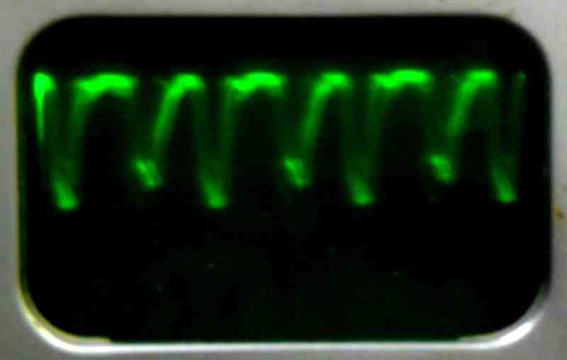
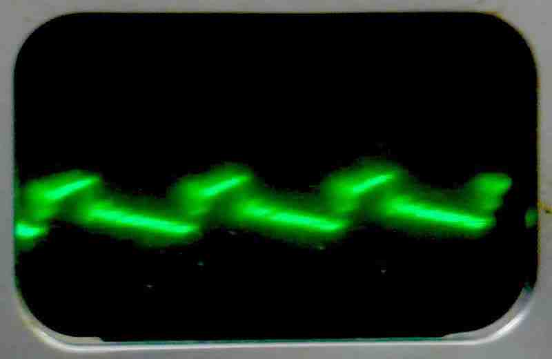
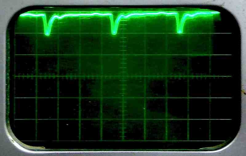
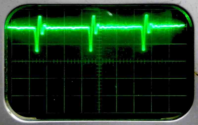
|
| Inhibit ripple at core and at supply
1µsec/div hoiz; 0.2v/div vertical | |
|---|---|
The high frequency component of the ripple measured at the supply output
is almost certainly an artifact of the feedback delay in the regulator circuit,
and it is noteworthy that this high frequency noise is invisible at the other
end of the several feet of
twisted pair
between the power supply and memory. What we do see at the other end is
a low-voltage echo of the supply current waveform we measured on
Apr. 18.
The relatively low resistance (or, at these frequencies,
impedance)
of the twisted pair translates the current waveform to the waveform we observed.
|
|
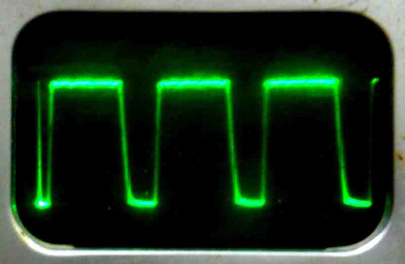
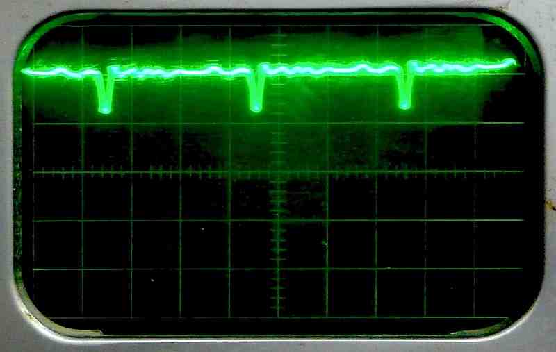
| R/W select ripple at core and at supply
1µsec/div hoiz; 0.2v/div vertical | |
|---|---|
As with the inhibit current, R/W select current ripple at the memory is higher aplitude and reflects the current waveform measured on Apr. 18. Unlike the case with the Inhibit current, however, we do not see the high frequency artifacts of the regulator circuitry at the power supply output, but just the same miniature version of the current waveform. This leads us to suspect that something in the R/W select supply is not working correctly.
Note that, when we reformed the power supply capacitors
(Bug 10), we found, on
Mar. 13, 2014,
that C15 was bad, and on
Mar. 27, 2014,
we installed a replacement.
C15 is the final (post regulator) filter capacitor for the inhibit supply,
while its twin, C16, is the final filter capacitor for the R/W select supply.
Both are nominally 980µF 75V electrolytic capacitors, although our
replacement is labeled 1000µF.
If C16 capacitor is bad, it would lead to poor power supply regulation,
but we also need to consider the possibility that the series regulator
transistors are bad or that one of the G808 boards that control them is bad.
Bug 64: To help rule out problems with the power supply regulation, we tried switching the power transistors Q1 and Q2 inside the power supply. These are big 2N3715 80V, 150W, 10A Silicon NPN transistors mounted on the power supply frame. Q1 regulates the Inhibit supply, Q2 regulates the R/W Select supply. See the power supply schematic in the Maintenance Manual (1965 ed, Drawing RS-C-708, page 10-8). Switching the transistors had no obvious effect on the ripple signal observed across the power supply output, although in switching the transistors, we did notice that one of the mounting screws for one transistor was not very tight. This could have added resistance to the current path.
We also tried switching the G808 regulator boards in the power supply. Given that the set point of each board is adjusted differently, we would not expect the machine to work with these boards switched, but we wanted to see if the quality of voltage regulation changed. It did not, so we switched the boards back.
Conclusion. The power supply electronics is not obviously bad.
| Read MC16 pin J |
|
| Strobe MD20 pin N |
|
| Inhibit Any G209 Pin E |
|
| Write Any G209 pin D |
|
| Mem Done MF36 Pin 1 |
|
Note that the Drawing BS-D-8M-0-13 in the Maintenance Manual shows Read and Write with filled-in diamonds as arrow heads. According to Figure 10-1, this notation indicates a negative level signal, that is, one where true is indicated with a negative voltage. Drawing BS-D-8M-0-15 shows Inhibit as a negative level.
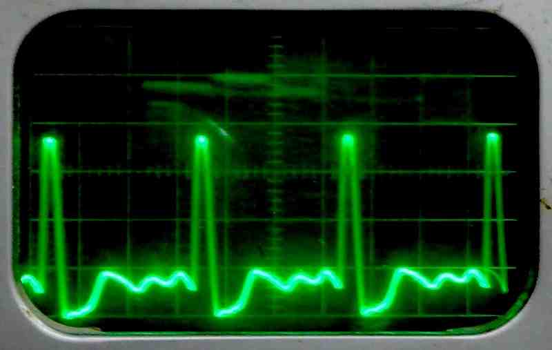
Two things look wrong here: First, the memory strobe amplitude looks too small. The scope shows a negative pulse with an amplitude of about 1.4V. The source of this signal is a B360 module. The 1967 Logic Handbook, page 122, says that the output is a 40ns negative pulse with an amplitude of 2.5 volts. Fortunately, the B360 board has been reverse engineered by Vince Slygstad. We must check if we are working with Rev C (7-65) or rev D (11-65), but he has produced schematics of both boards.
The second puzzle has to do with the Inhibit and Write signals. These should be very similar, and neither should be almost coincident with Read. Inhibit pulses should begin 50ns before Write and the two pulses should end as the Memory Done pulse begins. (Note that the scope traces for Read and Write are inverted relative to the signals shown in the maintenance manual because they are negative logic signals.) The strobe pulse does occur in the center of a 600ns read pulse, as expected, and the Write pulse is about 500ns wide, ending with the Memory Done pulse. Something seems wrong with Inhibit, since it does not end coincidently with Read.
Have we hooked the scope probe to the wrong signal or is it really bad?
Reviewing the schematics, particularly
Drawing BS-D-8M-0-13
in the Maintenance Manual shows that pin E of any G209 board is not Inhibit, it
is Read. We made a mistake.
|
We did not change the triggering or horizontal sweep rate on the scope from
the settings on Sept. 13", so the timing in those
scope traces is the same as the timings shown here. All of the scope traces
shown below were made with the zero reference 2 divisions above the center of
the screen.
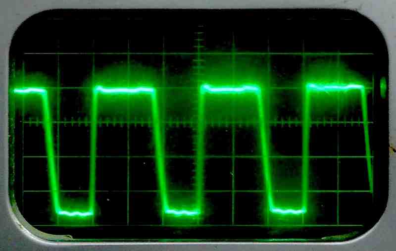
| Q4 base 1V/div |
|
| Q3 base 1V/div |
|
| Pin L 1V/div |
|
| Q1 collector 2V/div |
|
| Q2 collector 2V/div |
|
| Pin N 1V/div |
|
In sum, the B360 seems to be working, with no obvious explanation of the low amplitude of the output pulses other than the low impedance of the 12 sense amplifiers that it drives in parallel.
We have two obvious questions: First, is our scope calibration good? The DC voltages we measured with our multimeter on the various DC busses on the B360 don't match the mesaurements with the scope.
Second, the output of each sense amplifier is an and function of the strobe pulse and the pulse amplified from the sense winding of the core memory. If the timing of the delay line is wrong, nothing will get through.
Note added Oct. 4: All pulses shorter than 100ns should look undersized
on this scope! The advertised bandwidth of the
Tektronix 321
scope we are using is 5MHz. It's an analog scope, so it does show features
faster than 500MHz, but they are attenuated. So, the waveforms above are close
to what we should expect if the B360 board is working perfectly.
Bug 65: On July 2, 2015, we built some very simple logic probes for DEC's R-series logic. These have an LED that glows when the logic level is 0V, and is off at -3V. They work well for debuging static logic, but to continue debugging the machine, we need to examine fast pulses. This led us to design a more complex logic probe for fast pulse detection. In the end, this design was only a partial success, more on that later.
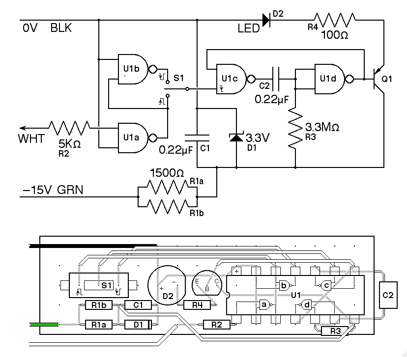
|
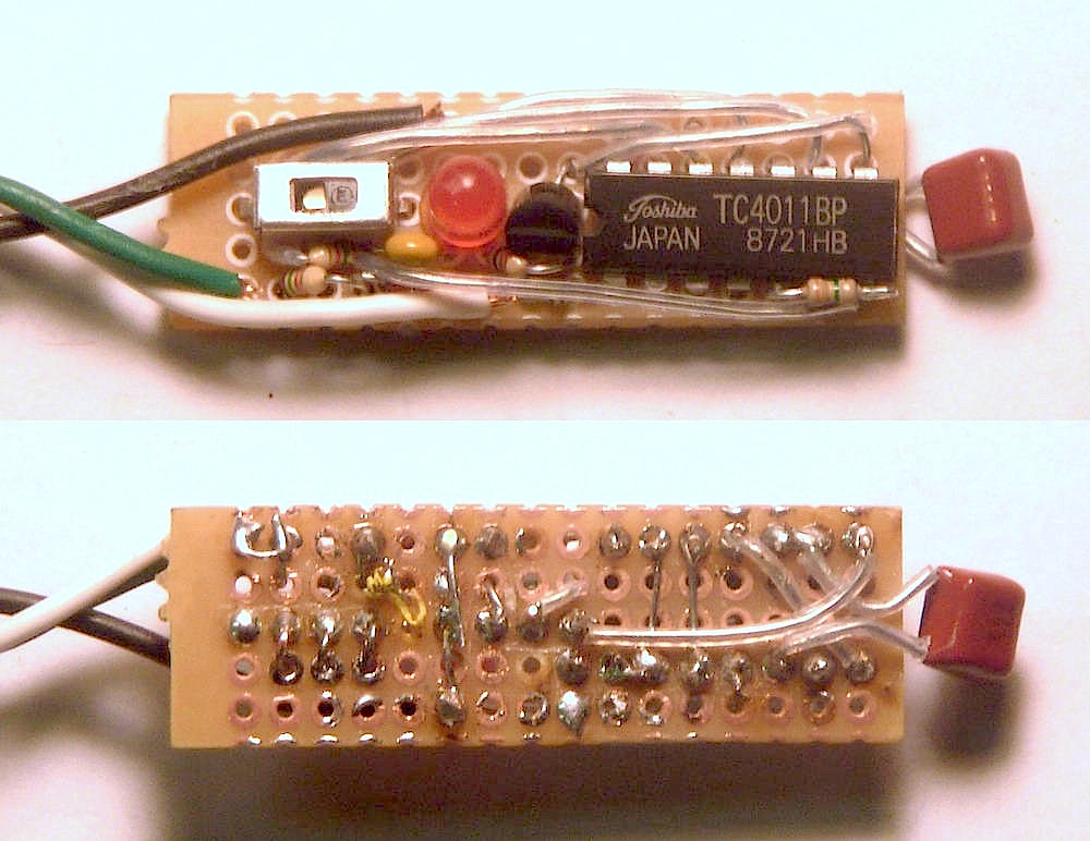
|
|
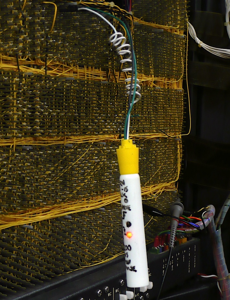
| Assembled | In use |
The photos to the right shows the entire probe circuit assembled on a sliver of protoboard, and then assembled in the casing of an old highlighter. The highlighter case was prepared by removing the plug from the base (it pulls out if you get a good grip on it with needle-nose pliers), pulling out the dry felt that formerly held the ink, scraping off the markings on the barrel and then drilling holes to align with the S1 and D2. It was difficult to push the circuit board into place and then insert twists of old vinyl cable sheath behind ti to wedge it into place. It turned out to be impossible to disassemble the probe without breaking off the switch handle.
Originally, we built this probe with the one-shot set up to make a 1 second blink. This was way too long, so we rebuilt it for a 1/2 second blink, replacing the large capacitor shown in the photo with a much smaller one.
The test leads were terminated with female Molex connector pins insulated with 1/8 inch shrink tubing. These pins fit nicely on DEC's wire-wrap backplane pins.
In testing, we found that this probe could easily detect 400 ns pulses and that it could usually detect 100 ns pulses. Pulse polarity matters for 400 ns pulses; the probe only reliably detects the leading edge of the pulse, not the trailing edge. This is because the one-shot has a recovery time after a wrong-polarity pulse determined by the RC time constant of C2 and the unknown resistance of the protection network on the CMOS logic input in parallel with R3.
This probe is totally blind to standard DEC R-series 40 ns pulses. Initially, we thought that the problem was too high a resistor protecting U1a, so we reduced this to 5 K&Ohm;. This was not sufficient, so we went back to the datasheets for the 4011 quad nand gate and found that the advertised gate delay of this chip grows quite long as the supply voltage falls below 5 volts. In sum, this was the wrong chip to use for a logic probe designed for work on DEC R-series logic, although it is fast enough to be useful with some of the slower timing signals in our machine.
We have one minor complaint about the probe: The electronics needs to be
shielded. As it is, just touching the case of the former highlighter will
sometimes trigger the one-shot.
Bug 64: We used two of the logic probes we built on July 2, 2015, plus the new probe we finished on Nov. 7, we traced the flow of data from the switch register (bit 11, the least significant bit) to the inhibit drivers.
The path is as follows:
We cannot look at the path from memory without a faster logic probe. All data
transfers from memory are very (40 ns) DEC standard R-series pulses
produced by the sense amplifier, which ands the memory strobe pulse with
the data from memory to produce the pulse that carries data to the memory buffer
register, directly setting each bit where a 1 should appear.
Bug 65: On Nov. 7, we described a logic probe that was almost useful, except that it was insensitive to the fast pulses used in DEC R-series logic. The fundamental problem was that the 4000 family of CMOS logic is too slow. We designed a new logic probe using 74HC series CMOS logic, which is much faster. While we were at it, we also increased the number of LEDs to 3, green for high (0V) inputs, red for a low (-3V) inputs, and orange for edges. CENTER
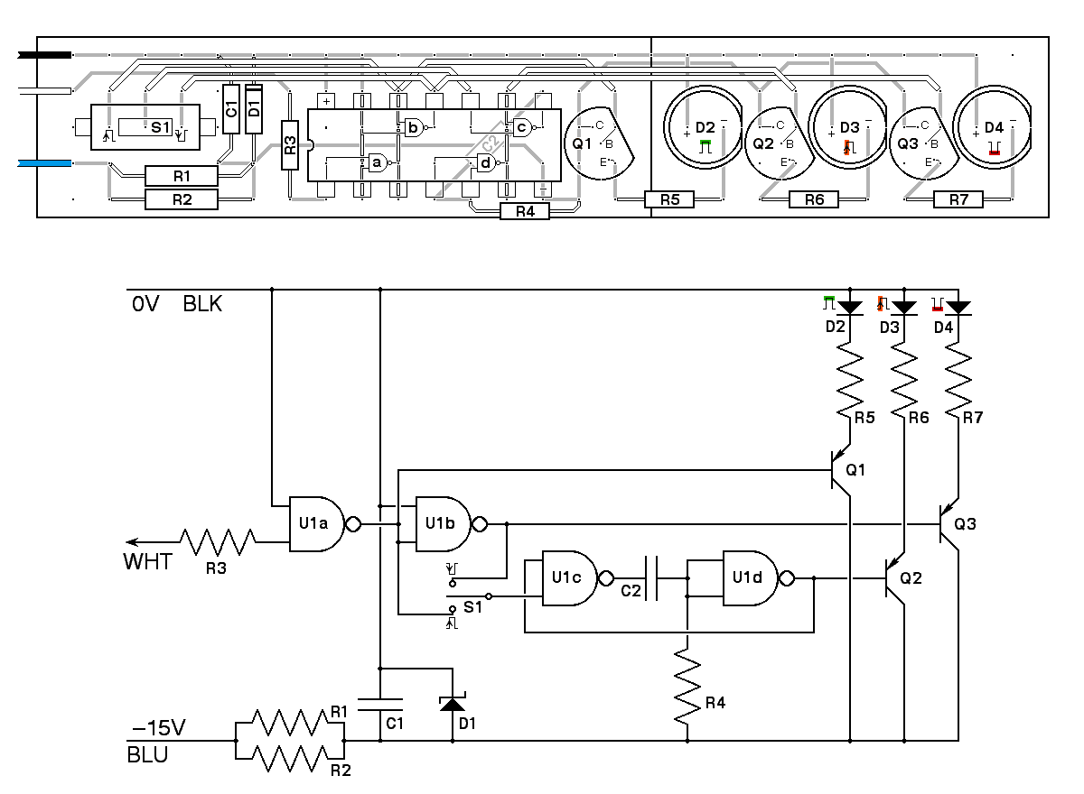
|
The parts used for D2, D3 and D4 were constrained by what was available in the inventory of the enginerring electronics shop. They are all T-1 3/4 LEDs, although the red LED was shorter and required a shim to sit at the same height as the others. All have a forward voltage around 2 volts at 10mA, but we are operating them at a lower current.
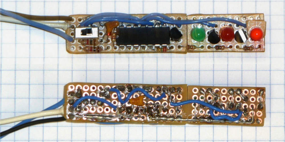
|
| The assembled probe |
In use, the probe's input impedance is so high that all three lights come on when the input wire isn't connected. That's because it's picking up everything from 60 cycle hum to RF noise. It settles down and behaves nicely when connected to something.
Bug 64:
In testing, the new logic probe worked well, and was reliably able to detect
70ns pulses.
Unfortunately, it still does not detect the 40ns memory strobe pulse. We think
this pulse may really be under-height — that is, the 1.5V amplitude
observed on Sept. 27, 2018 may be real and not an
artifact of the scope's low bandwidth. We need to take out some of the
sense amplifier boards to see if one or more of them have shorted diodes that
pull this signal to ground.