8. Arithmetic and Logic.
Part of
22C:40, Computer Organization and Hardware Notes
|
19th century logicians, most notably George Boole, identified the basic operators of what we now know as Boolean logic, the and, or and not operations. These operators are, of course, the familiar operators used in Boolean expressions in common programming languages as well as being the basic operators of the logic that philosophers have studied for millenia. What logicians like Boole did was bring these into the realm of mathematics by demonstrating that these operators formed an algebra in just the way that addition and subtraction on the integers form an algebra.
Boolean logic operates on the values true and false, and it was George Boole who recognized that if true is represented by the value one and false is represented by the value zero, we can think of the or operator as being similar to addition, where adding zero to a value leaves that value unchanged, and the and operator can be thought of as being similar to multiplication, where multiplying a value by zero always gives zero, and multiplying a value by one leaves that value unchanged.
The field of Switching theory emerged before World War II, largely motivated by the use of complex systems of electromechanical relays in telephone exchanges. This field applies Boolean logic to practical engineering problems, and with the development of electronic calculators and then computers, switching theorists quickly moved into the center of certain aspects of computer design.
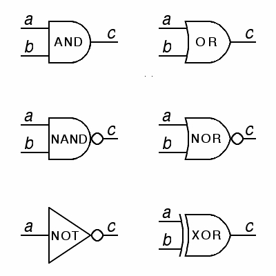
Engineers in general and electrical engineers in specific have a long tradition of using graphical notations to do their design work, and by the late 1960's, a standard graphical notation emerged for Boolean logic that is well suited to the problem of expressing the uses made of this logic formalism in the context of computer design. The basic elements of this notation are given here:
|
|
| inputs | the output c | |||||||
| a | b | AND a b | OR a + b | NAND a b | NOR a + b | NOT a | XOR a ⊕ b | |
| 0 | 0 | 0 | 0 | 1 | 1 | 1 | 0 | |
| 0 | 1 | 0 | 1 | 1 | 0 | 1 | ||
| 1 | 0 | 0 | 1 | 1 | 0 | 0 | 1 | |
| 1 | 1 | 1 | 1 | 0 | 0 | 0 | ||
The algebraic notation shown in the above table is an adaptation of the notation originally proposed by Boole, who used multiplication and addition symbols for the and and or operators. The use of the overbar to mean not emerged later, as did the use of the circle around the plus symbol to mean exclusive or.
In addition to the conventional Boolean operators and, or and not, engineers quickly introduced two new operators, nand and nor. These correspond to and and or with their results inverted by a not operator, as indicated in the algebraic notation for Boolean logic by an overbar over the expression. These were introduced largely because the simplest amplifiers used in digital logic perform the not function, and a typical hardware implementation of the and or or function produces an output that must be amplified before it is used as an input to another logic operator.
The triangle symbol is an old symbol for an amplifier in electronic schematics, and it is still used in this way in some schematic diagrams for logic circuits, standing for a gate with inputs and outputs that are equal. The small circle on the output of the nand, nor and not gates indicates logical negation. Conventionally, this is placed on the output of the gate, but occasionally, you will see this little circle placed on an input in order to indicate the presence of an inverter or not gate built into that input.
The exclusive or operator is also given a special symbol in this schematic notation, but not because it is a primitive operator that is easy to build in hardware. In fact, the exclusive or operator is difficult to built, requiring hardware equivalent to 4 nand operators, but it is very common in arithmetic.
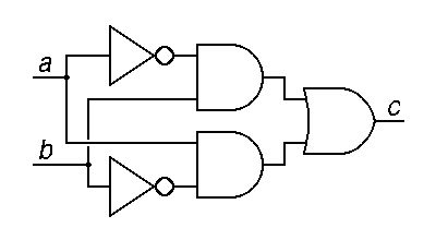
Electrical engineers refer to hardware devices that perform the functions of Boolean operators as logic gates. Each physical logic gate has connections for a power supply as well as connections for inputs and outputs. A schematic diagram shows the interconnection of inputs and outputs as lines between the symbols for the individual gates; these are frequently referred to as wires, even if the actual hardware involves conductive traces on silicon or on a printed circuit board. The following collection of simple gates, for example, are shown connected to perform the exclusive or function:
|
| c = a ⊕ b = (a b) + (a b) |
When explaining the exclusive or function, there are several reasonable explanations. For example: The exclusive or is true if one of the inputs is true and the other is false. The formulation given in the figure above, in both schematic and equational forms, corresponds to the this Englis explanation. Alternatively, the exclusive or function is true if one or the other input is true, but not both.
It is worth pointing out some notational convention from schematic diagrams used by electrical engineers. First, unless other considerations demand changes, inputs are usually on the top or left side, and outputs are usually on the bottom or right side. Second, where wires cross, this may be indicated by a schematic indication that one wire hops over the other, while where wires are connected, a dot is added to emphasize the connection. Furthermore, connections are usually shown with lines meeting to form a T, while intersections form an X.
Engineering students have been required for several decades to buy a template for drawing the symbols for the logic gates, since freehand drawings can be quite sloppy. If you do draw them freehand, note that the key features that distinguish an or symbol from an and symbol are as follows: The or has a curved input side and a slight point on the output side, while the and has an input side that is straight and an output side that is a perfect half-circle.
Exercises
a) Consider the logic diagram given above for constructing an exclusive or gate from and, or and not gates. What function does this compute if 3 nand gates are substituted for the 3 two-input gates used in the diagram? The easy way to solve this is to work out the truth table for this modified circuit by brute force, tracing the values of each intermediate point for each of the 4 possible combinations of inputs.
b) Consider the logic diagram given above for constructing an exclusive or gate from and, or and not gates. What function does this compute if the 2 not gates are replaced by a single nand gate that combines the a and b inputs and passes its result to both of the inputs originally served by separate not gates.
c) Consider the problem of comparing two 1-bit binary numbers for equality. This can be done with an exclusive-or gate and one other gate to give an output of 1 if the numbers are equal and an output of zero if they are different. Draw the schematic diagram for a a solution to this problem and give an equation in Boolean logic notation.
It is easy to see how each bit of a binary number can be associated with a value from Boolean logic, and George Boole's convention that 1 is used to represent true and 0 is used to representfalse extends quite naturally to the representation of binary numbers on a computer as vectors of Boolean values. Thus, we can think of the 32-bit binary number a as being composed of a vector of boolean values a0 to a31, where the subscripts incicate the power of two in the place-value system.
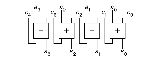
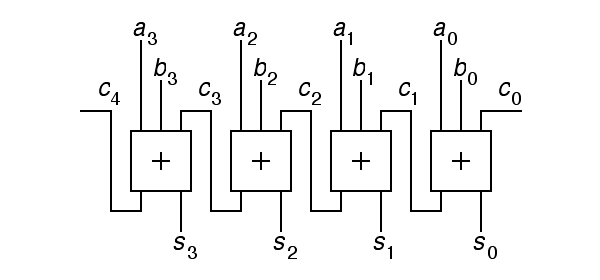
Given such a number, how can we build hardware to perform arithmetic operations on it? For example, how can we increment this number? To answer this, it is useful to step back and review how we increment a number by hand. We add one to the least significant digit, and if the result is greater than the radix, we add one to the next digit; we call this operation adding the carry to the next digit. From this, we conclude that there is a local operation we are performing at each digit, and that this operation must compute not only the output value for that digit but the carry that is to be added to the next digit. In schematic terms, we have the following:
|
In the above diagram, the 4-bit addend a is incremented to produce the 4-bit sum s. The carry bits c violate our standard convention for the direction of data-flow, left to right and top to bottom, because we have allowed our convention for writing numbers to force the least significant bit to appear on the right side. The carry in to the entire incrementor is c0. If this is zero, the sum s will be equal to the addend a, while if it is one, s will usually equal a. The intermediate carry bits c1 to c3 hold the carry out of one stage of the incrementor and into the next. The final carry bit, c4 holds the carry out of the adder; if this is one, the input must have been 1111 and the output is 0000, an unsigned overflow.
The logical operation performed at each bit position in the above incrementor, within the box marked with a plus sign, is fairly simple. There are two inputs, ai and ci, and two outputs, si and ci+1, so the truth table for this function will have 4 rows and two output columns. Here it is:
| inputs | outputs | |||
| ai | ci | ci+1 | si | |
| 0 | 0 | 0 | 0 | |
| 0 | 1 | 0 | 1 | |
| 1 | 0 | 0 | 1 | |
| 1 | 1 | 1 | 0 | |
The above truth table was filled in by counting the number of one bits in the input row and then recording the sum of those bits, as a binary value, in the output row. The least significant bit of this sum is the sum output for that bit position, while the most significant bit of the sum is the carry into the next bit position. Having built the table, it is easy to compare each output column with the outputs of the various standard Boolean functions. On doing this, we see that ci+1 is just the logical and of ai and ci, and that si is the exclusive or of ai and ci. This leads to the following gate-level design for each digit of the incrememtor:
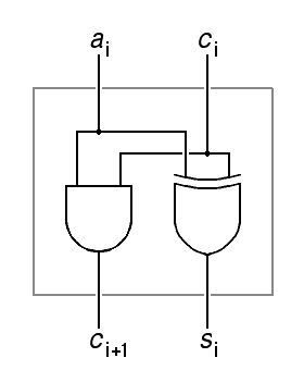
| ||||
| ci+1 | = | ai ci | ||
| si | = | ai ⊕ ci | ||
Exercises
d) Work out the truth table for decrementing a binary number, with inputs ai (a digit of the number to decrement) and bi (the borrow input to that digit position) and outputs bi+1 and di (the decremented output). Then follow through and give a gate-level schematic for one bit of an incrementor. Note that bi will be true when one is to be taken from ai and false when one is not to be taken away.
e) From simple algebra, a-1 is -((-a)+1), and further, -x is x+1 in the two's complement system. Therefore, we can build a decrementor from an incrementor with some added inverters. Show the logic diagram for this!
Having met with success in designing an incrementor, we can attempt to use the same approach to design an adder. As with incrementing, addition involves propagation of carries from one digit position to the next, but instead of a single input, we have two inputs, the addend, which we will call a and the augend, which we will call b. (Yes, addition is commutitive, so we could call them both addends, but the terms addend and augend are available in English to distinguish the number that is added to from the number added to it.) At the top level, a 4-bit adder will look like the following:
|
The truth table for one bit of an adder is very similar in form to that for one bit of the incrementor, but it has 3 inputs instead of two. As with the truth table for the incrementor, we can read each two-bit output row as a binary number giving the number of one bits in the corresponding row of the inputs, but now, our sums run from zero to three instead of having a maximum value of two. Here is the table for the adder:
| inputs | outputs | ||||
| ai | bi | ci | ci+1 | si | |
| 0 | 0 | 0 | 0 | 0 | |
| 0 | 0 | 1 | 0 | 1 | |
| 0 | 1 | 0 | 0 | 1 | |
| 0 | 1 | 1 | 1 | 0 | |
| 1 | 0 | 0 | 0 | 1 | |
| 1 | 0 | 1 | 1 | 0 | |
| 1 | 1 | 0 | 1 | 0 | |
| 1 | 1 | 1 | 1 | 1 | |
While the above truth table resembles that for the increment function, and in fact, while the first 4 rows of the output are the same, it is complex enough that it is not easy to see how to derive the outputs from the inputs using any simple logic functions. There is a way!
Focusing only on the sum output si, this output is one only when an odd number of ones appear in the corresponding input row; furthermore, so long as any one of the inputs is zero, this output is the exclusive or of the other two inputs. In fact, si=ai+bi+ci if we use the plus sign to mean the exclusive or operator. (We do not need to parenthesize this expression because evaluating these operators in any order always leads to the same result.)
Focusing on the carry output ci+1 shows a more complex pattern, but with a bit of thought, it is not difficult to determine that ci+1=(ai&bi)|(ai&ci), using the & and | operators to stand for and and or as they do in languages like C and Java.
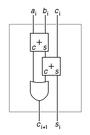
From this ad-hoc reasoning, we can conclude that our adder is composed of two incrementors plus an additional or gate to combine the two carry out lines. This is why our increment circuit is frequently called a half adder and our adder is distinguished from the incrementor by calling it a full adder. This is illustrated in the following figure:
|
Ad-hoc design is a slow and labor intensive process, and if we want to build interesting computers without taking centuries, we need a systematic approach to designing logic circuits that implement arbitrary Boolean functions. Switching theory, a field that began to develop in the 1920's motivated by the development of the dial telephone system, is a field that combines this practical interest in engineering with the abstract mathematics of Boolean logic.
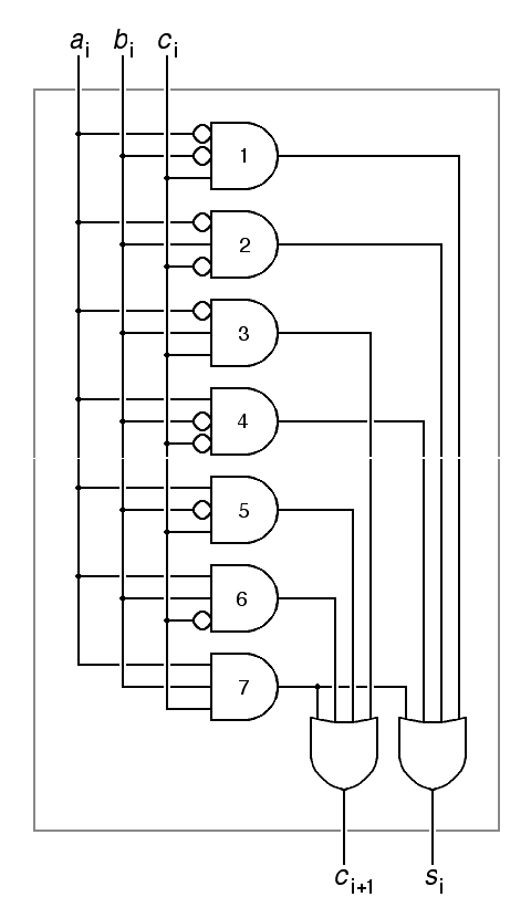
Switching theorists have come up with the following general methodology for converting any truth table to a logic circuit to compute the Boolean function described by that truth table:
- Arrange a column of and gates, one gate per row of the truth table but only for those rows where the output section of the truth table is not all zeros. Number these and gates using the row-numbers in the truth table, where the row number is obtained by reading the input values for that row as a binary number. The and gates have their inputs on the left and their outputs on the right.
- Arrange a row of or gates below and to the left of the and gates, using one or gate per output of the function. The inputs to these gates are on top, and their outputs are on the bottom. Label the outputs in the same order they are in the truth table.
- Arrange the inputs in a row above and to the left of the column of and gates, and for each input, add an inverter so that both the input and its inverse are available.
- For each of the and gates, wire its inputs according to the ones and zeros in the corresponding row of the input half of the truth table. The input half of the truth table is sometimes known as the and array because of this! If there is a one for some input in that row, that input should be connected as an input to that gate. If there is a zero, the inverse of that input should be connected as an input to that gate. Each of these and gates will have an output of one only when the inputs are set to the binary code for that row.
- For each of the gates in the row of or gates, wire it according to the ones in the corresponding column of the output half of the truth table. The output half of the truth table is sometimes known as the or array because of this! For each one at the intersection of a row and column in the output half of the truth table, wire the output of the and gate for that row to the input of the or gate at the base of that column. This completes the circuit!
The circuit below illustrates the use of the above methodology to implement a full-adder:
|
We have made one common notational compromize above! Instead of cluttering our diagram with inverters for each input to the full-adder, we have simply used small circles on the inputs to the and gates to indicate the need to wire that input to the inverse of the corresponding input instead of to that input. This allows us to read off the binary representation of the row number from the inputs of each gate, reading the circle standing for an inverted input as a zero and the circle standing for an un-inverted input as a one.
Exercises
f) Show the truth table for a subtractor that computes d=a-b, with borrow signals connecting each digit position to the next. The top-level schematic view of this subtractor will look identical to the top-level schematic view of the adder, but it will subtract. Now, answer this auxiliary question: What function does this compute when the borrow input to the least significant bit is true?
g) Draw out the gate-level schematic view of an adder given above, using explicit not gates instead of bubbles on the inputs to the and gates. Note: This can be done with exactly 3 inverters, since no input needs inversion more than once!
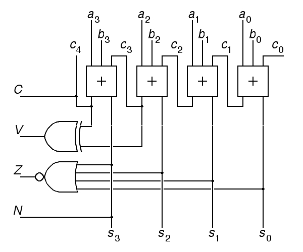
It is reasonable, at this point, to consider how the condition codes are computed. This computation is remarkably simple! Because the Hawk is a two's complement machine, we can simply treat the most significant bit of the sum as the sign bit and make a copy of this as the N condition code.
The Z condition code should be set of every bit in the sum is zero. Equivalently, Z should be reset if any bit in the sum is nonzero. The equivalence of these two formulations follows from DeMorgans laws:
| a + b | = | a b |
| a b | = | a + b |
As a result, we can use a multi-input nor gate to combine all of the bits of the sum to produce the Z bit of the condition codes.
The C bit is simply the carry out of the most significant bit of the adder, but V, the overflow bit, is a bit more difficult to work out. There are several ways of thinking about overflow detection. For example, we could declare an overflow if the signs of the addends are the same and the sign of the result is different. This would require comparing two signs, which we can do with an inverted exclusive-or gate, and then using a second exclusive or gate to compare the sign of the sum with the sign of one or the other addend. It turns out, however, that there is a simpler rule: There is an overflow if the carry in to the sign bit of the number differs from the carry out of the sign bit. This is the form used in the logic diagram given here:
|
This schematic diagram violates the standard assumptions we are using for drawing such diagrams! Inputs were supposed to be on the top and left and outputs on the bottom and right, so that data flows from left to right and top to bottom. Here, we have the carry input c0 on the right and all 4 condition codes as outputs on the left. We do this because all but one of the condition codes report on things that concern the most significant bit of the sum, while the carry input concerns the least significant bit, and we have written the bits with the least significant bit on the right, in just the way we would write a binary number.
Exercises
h) Here is a Boolean expression in the notation of C and Java: !(!(a&&b)&&!(c&&d)). Use DeMorgan's laws to eliminate all of the negations from this expression and express it purely in terms of and and or operations. Also, draw both the original and the final expression using schematic notation with logic gates.
i) There are several other ways of computing the overflow condition code! Consider, for example: There is an overflow when the signs of the operands are the same but the sign of the result is different. Express this as a truth table, assuming a 4-bit adder, so the inputs are a3, b3 and s3. Reduce this truth table to logic gates (hint: It can be done with 2 exclusive or gates and some inverters.)
j) Draw the part of the schematic diagram for the derivation of the condition codes that pertains to the Z condition code, but without using DeMorgan's laws in the computation of that condition code.
We can use a simple adder for the arithmetic involved in indexed addressing, but what we really want at the heart of our central processing unit is a general purpose block of logic gates that can both add subtract, as well as performing other operations. This is called an arithmetic logic unit or ALU because, usually, the operations of Boolean logic are included among the operations this unit can perform.
How do we take our adder and extend it so that it can perform other operations? First, note that addition sits at the heart of the subtraction operation if we use two's complement arithmetic. So, instead of building a special subtraction unit, we can subtract by adding the two's complement plus one. Furthermore, the carry in to the adder can be used to add that extra one, so we do our subtraction by adding the one's complement with a carry in of one.
Next, note that a ⊕ 0 = a while a ⊕ 1 = a; this means that we can use the exclusive or operator to select between a logical value, a in this case, and its inverse a. This leads to the following design for an adder-subtractor:
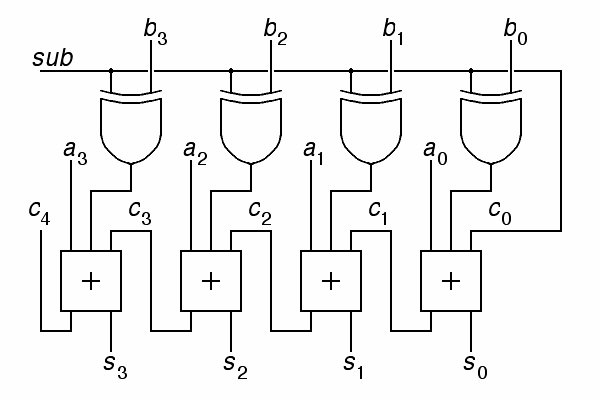
|
Here, if the sub input is zero, input b is not inverted and c0, the carry in to the adder, is zero, so the adder computes s=a+b+0. On the other hand, if the sub input is one, input b is inverted and c0 is one, so the adder computes s=a+b+1 which is a-b, the difference.
But, we need more operations. Looking at the set of operations supported by the C programming language, for example, we find not just addition and subtraction, but a much longer list that includes and, or and exclusive or as well a shift operators and more advanced arithmetic operators such as multiply and divide. We will ignore multiply, divide and floating point for now, and concentrate on the simpler of these operators.
Modern hardware designers build highly optimal arithmetic logic units to perform these, but we are not interested in optimal design here. What we want is a simple circuit that allows us to select between multiple functions depending on a control input. In this case, we need to select between addition and subtraction, on the one hand, and the and, or and exclusive or logical operators on the other hand. This is a total of 4 alternatives.
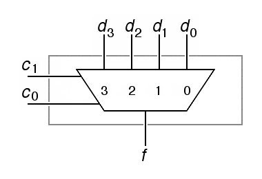
A logic circuit that has its output equal to exactly one of several sdata inputs depending on a control input is called a multiplexor, abbreviated MUX. The truth table for a multiplexor with 2 data inputs d0 and d1 and one control input c is as follows:
| inputs | f | |||
| c | d0 | d1 | ||
| 0 | 0 | 0 | 0 | |
| 0 | 0 | 1 | 0 | |
| 0 | 1 | 0 | 1 | |
| 0 | 1 | 1 | 1 | |
| 1 | 0 | 0 | 0 | |
| 1 | 0 | 1 | 1 | |
| 1 | 1 | 0 | 0 | |
| 1 | 1 | 1 | 1 | |
The above truth table reduces to a logic circuit that is quite simple, involving only 4 gates:
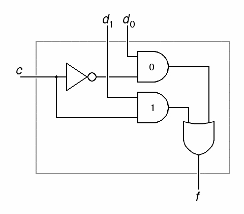
|
|
| f = (d0 c) + (d1 c) | |
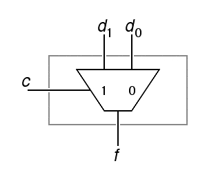
In complex digital systems involving many multiplexors, it is common to use the abbreviated notation shown at the right above. The trapezoidal shape has been used, historically, for any logical function that combines multiple inputs to produce one output, with the nature of the combination controlled by control signals coming into the slanted edge of the box, but the use of this symbol for functions other than multiplexing is in decline, and the numeric labels inside the box make it clear that one specific input is selected when the control input matches the label.
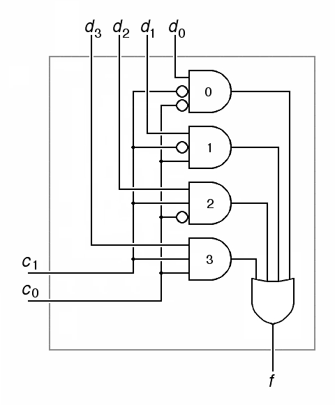
A 4-input multiplexor has 4 data inputs, d0, d1, d2, and d3, and 2 control inputs, c0, c1. The pattern of this logic is very similar, and is given below:
|
|
| f = (d0 c1 c0 ) + (d1 c1 c0 ) + (d2 c1 c0 ) + (d2 c1 c0 ) | |
In the gate-level version of the 4-input multiplexor given to the left above, the drawing uses the abbreviated notation that we used previously for inverters. There are 4 inversion bubbles in the figure, but if we used explicit inverters, we would only use 2 of them, one for each control input. In the abbreviated graphical notation given on the right, it is up to the reader to understand that the labels 0, 1, 2 and 3 inside the multiplexor symbol correspond to 00, 01, 10, and 11 on the control lines, where c1 is the most significant bit and c0 is the least significant bit of the control input.
We now have enough parts to build a basic arithmetic logic unit. This unit combines an adder-subtractor with three simple logic gates, using a multiplexor to select between the 4 functions. It would clutter the page too much to draw a full 4-bit arithmetic logic unit, but we can draw just one bit of this unit, with data inputs ai, bi and ci, data outputs si and ci+1, an f2 input to control the add-subtract function of the adder, and two more control inputs f1 and f0, used to control the multiplexor that selects between the arithmetic and logic functions.
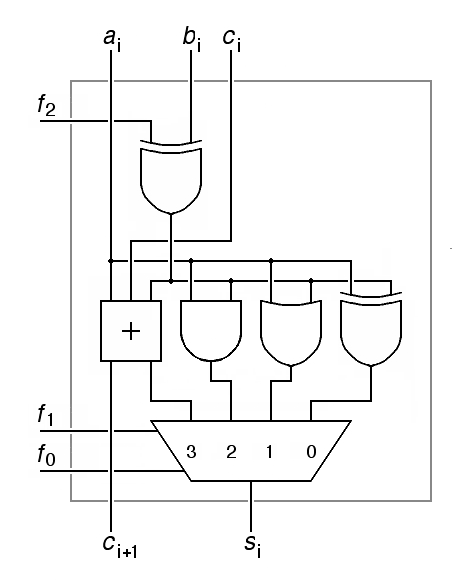
|
We call this a bit slice of the arithmetic logic unit. The full arithmetic logic unit for a machine like the Hawk would require a total of 32 such bit slices.
It should be noted that a high-performance arithmetic logic unit would rarely be constructed as shown here! There are two major categories of optimization that are typically pursued. First, the carry path through the arithmetic logic unit is almost always carefully optimized, so that carry propagation from the carry in to the least significant bit to the carry out from the most significant bit is far faster than is suggested by the designs given here.
The second common optimization is to make the adder itself compute the exclusive or function instead of using a separate gate for this, and to replace exclusive or gate used for the add-subtract function with a more complex bit of logic that takes both ai and bi as inputs, as well as two more control inputs, f0 and f1, thereby eliminating the multiplexor on the output of the adder.
Exercises
k) In the adder-subtrtactor, the carry output means carry, exactly, when the circuit is used for addition. When the circuit is used for subtraction, however, the situation is a bit muddy. What is the value of the carry output when the high bit of the subtractor outputs a borrow request and when the high bit of the subtractor does not output a borrow request?
l) Naive students frequently assume that the borrow signal should flow from more significant places in the subtractor to less significant places because when you borrow one, you take one from a more significant place and give it to a less significant place. Explain why this is wrong!
m) Explain why replacing the and and or gates in the 2-input multiplexor given above with nand gates is an example of the application of DeMorgan's laws.
n) Another way to build a 4-input multiplexor is with a binary tree of 2-input multiplexors. Draw the schematic diagram for this tree, and then estimate the number of and, or and not gates required to build this tree and compare this with the 7 gates required to build the 4-input multiplexor directly. Can you give corresponding figures for an 8-input inverter built using this binary tree approach compared to an 8-input inverter built directly?
o) The bit-slice of an arithmetic logic unit given above has 3 control inputs, f2, f1 and f0. Therefore, it can compute 8 distinct fuctions of its a and b inputs. List them, and then go throught the Hawk instruction set and figure out which register-to-register instructions on the Hawk use each of these functions. Ignore memory-reference instructions; they don't use the arithmetic logic unit; indexed addressing is done using a separate adder.
In addition to arithmetic and logic operations, most computers and many programming languages support shift operators. For example, languages descended from C, such as C++ and Java, include the operators >> meaning shift right and << meaning shift left. The effects of these operators are illustrated below:
| expression | value | |
|---|---|---|
| binary | decimal | |
| i | 00001000 | 8 |
| i >> 1 | 00000100 | 4 |
| i >> 2 | 00000010 | 2 |
| i >> 3 | 00000001 | 1 |
| i << 1 | 00010000 | 16 |
| i << 2 | 00100000 | 32 |
| i << 3 | 01000000 | 64 |
Shifting is included in the instruction set for two distinct reasons. First, it allows moving bits around, for example, to extract successive bits from a word for transmission over a serial data line, or to pack multiple 4-bit data items into a word. The second reason is apparent when you examine the decimal equivalent of the binary values in the example above! Shifting left c places is equivalent to multiplication by 2c and shifting right c places is equivalent to division by 2c.
A hardware device that takes an n-bit number as input and shifts that number c places is called a shifter. Clearly, there are two types of shifters, left-shifters and right-shifters. A shifter for an n-bit word can be made from n multiplexors, where the number of inputs per multiplexor determines how many different values of the shift-count c the shifter can handle. Here is a 4-bit shifter:
|
We have made some notational compromize above. In order to save space, we have drawn the multiplexors touching each other at the corners. This is bad form generally, but in this context, it does not lead to confusion. Generally this should not be done unless the control inputs to all of the multiplexors are provided by the same source, so they operate in parallel. That is exactly the case here, and that is the source of a second notational compromize: We have connected the shift-count inputs directly to the leftmost multiplexor, and then implied, rather clumsily, that the control inputs to one multiplexor are passed on to the next sequentially. These kinds of notational compromizes are fairly common in hand-drawn diagrams of computer logic.
The shifter shown above computes s = d >> c; that is, it shifts its 4-bit input left from 0 to 3 places. This poses an interesting question? What value should be "shifted into" the output for bits that were not part of the input number? In the above, this value is provided by an auxiliary input, d4. For left-shift operations, the usual answer is to shift zeros in from the left, so that the result is the result you would expect for multiplication by 2c.
For right-shift, there are two useful answers. First, we could shift in zeros, as with left-shift; in this case, the result will be the correct result for division by a power of two, assuming that the input number was treated as an unsigned integer. This is called a logical right shift or an unsigned right shift. The other alternative is to shift in copies of the sign bit. For the 4-bit shifter shown above, this would involve connecting the d4 input to d3. In this case, if the input is a two's complement binary number, the output will be the correct two's complement result for division by a power of two, with one very important exception! If the quotient is not exact, that is, if there is a nonzero remainder after division, the result will be rounded to the next lower integer instead of being rounded toward zero. As a result, -5>>1 is -3, not -2. This is called an arithmetic right shift or a signed right shift.
It is worth noting that in C and C++, when you declare a variable to be of type int and then apply the >> operator to it, this usually implies a signed right shift, while if you declare the variable to be of type unsigned int and then apply the same operator, this usually implies an unsigned shift. In contrast, in Java, where the built-in integer type is signed and there is no way to declare an unsigned integer, the language supports two distinct right-shift operators, >> and >>> to distinguish between these two alternatives.
The Hawk machine has both left and right shift operators, and the right shift operators are available in both signed and unsigned form. One feature of the Hawk machine that separates it from many other machines is that the shift operators are combined with a variant of the add instruction, so that, in one instruction, a number can be shifted and added to another number. The Hawk instructions for this are ADDSL, ADDSR and ADDSRU (the latter being the unsighed right shift). To accomodate these shifted versions of the add operation, there is a right-shifter on the output of the Hawk arithmetic logic unit and a left-shifter on one of the inputs of the Hawk arithmetic logic unit.
As with the discussion of arithmetic logic units, the design of shifters used in real computers is frequently more complex than that given here. The primary problem with the approach given here is that a 32-bit shifter with a 4-bit shift-count would take 32 multiplexors with 16 inputs each! In designing computers, it is common to avoid using extravagant amounts of silicon for rarely used functions, and in the case of shifters, the solution is to use a shift tree, also called a barrel shifter, where one stage of the shifter shifts only a short distance, say 0 to 3 bits using a 2-bit shift count, while the next stage shifts in multiples of 4, again using a 2-bit shift count. As a result, we can achieve exactly the same shift function with 64 4-input multiplexors instead of 32 16-input multiplexors.
Exercises
p) Draw the diagram for a 4-bit left shifter able to shift from zero to three places.
q) Draw the diagram for a 4-bit right shifter composed of a cascade of two levels using 2-bit multiplexors at each level, where the top level shifts either 0 places or 2 places, while the second level shifts either 0 places or 1 place. Make sure to label the inputs and outputs so that they are exactly compatable with the 4-bit shifter illustrated above.
r) Explain how the Hawk EXTB instruction is implemented using eight 4-input multiplexors. What bits of what register(s) are used to control these multiplexors? What bits of what register(s) are used as inputs to these multiplexors?